Differential Amplifier (TSMC 65nm)
Cadence Virtuoso
Spectre
Analog IC Design
Layout
DRC/LVS
Tapeout
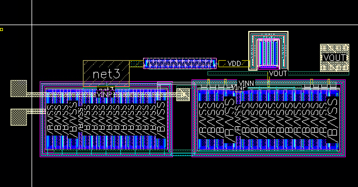
Designed transistor-level differential amplifier system in TSMC 65nm CMOS meeting gain (>26 dB), power (<500µW), and output swing (>300mV) specifications.
System Architecture:
- 4-bit digital address decoder (NAND logic) enabling device when address matches 1011
- Low-threshold transmission gate switches for bus isolation
- NMOS differential pair with active PMOS load and tail current mirror
- Sub-40nA standby current when disabled, ~220µA active quiescent current
Performance Achieved:
- Open-loop gain: ~28 dB @ 1 MHz (spec: >26 dB)
- Power consumption: ~264 µW (spec: <500 µW)
- Output swing: ~418 mV peak-to-peak (spec: >300 mV)
- Switch Ron: ~76 Ω (spec: <100 Ω)
- Switch Roff: ~16.7 MΩ (spec: >10 MΩ)
- Digital decoder delay: ~249 ps (spec: <500 ps)
Layout & Verification:
- Common-centroid layout for differential pair to minimize DC offset mismatch
- Hierarchical design flow with biasing network
- Upper metal layer routing (M7, M8) with orthogonal direction policy to suppress parasitic cross-coupling
- Full DRC and LVS verification completed
- Sent to TSMC for fabrication
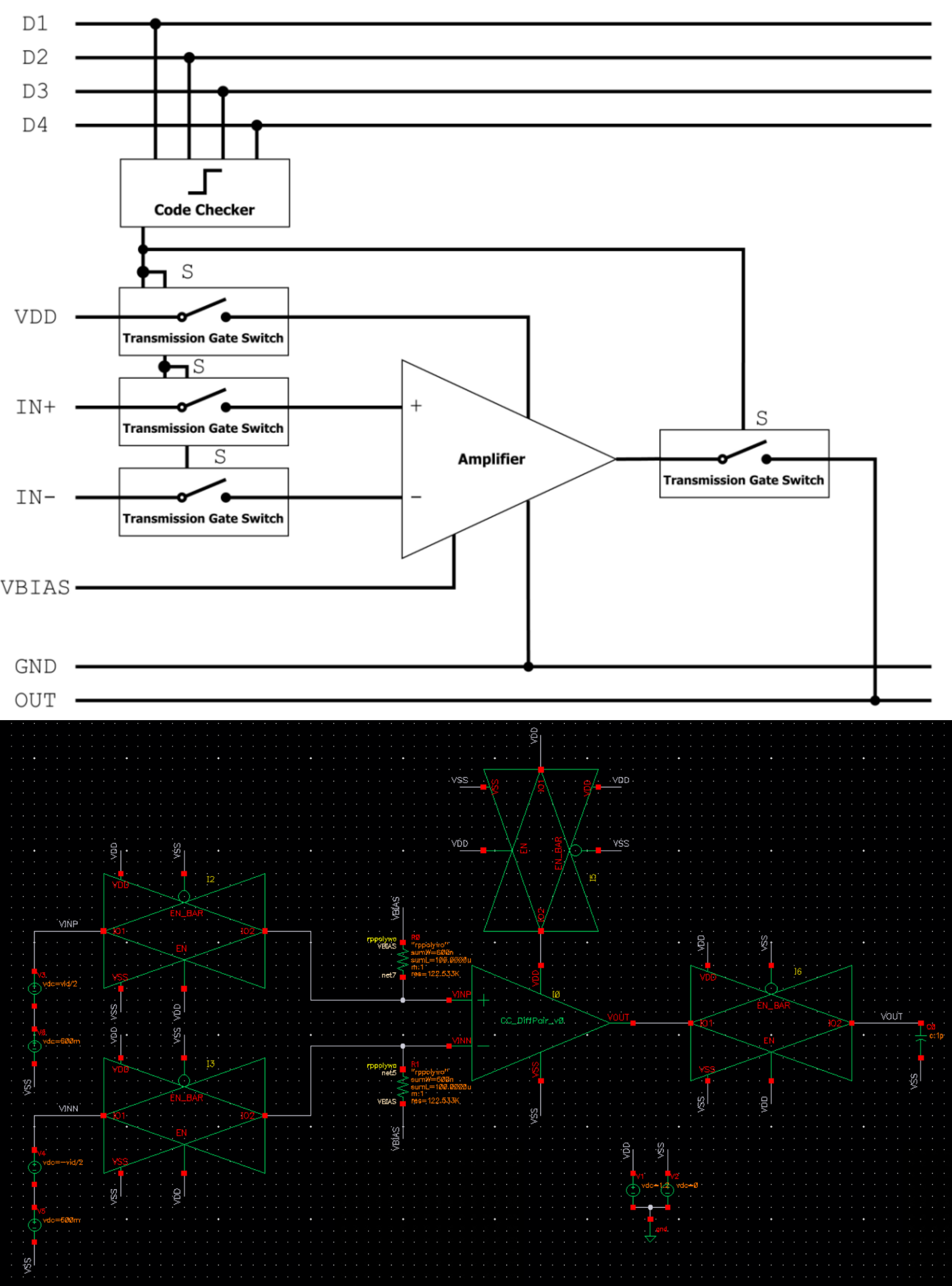
Complete system architecture block diagram & schematic
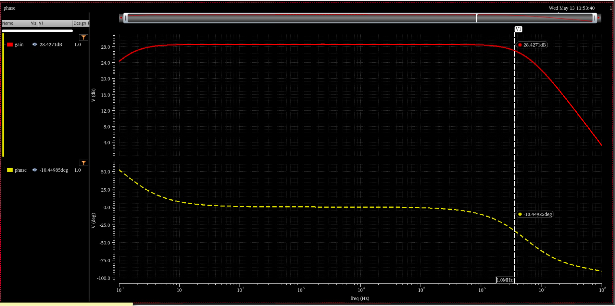
AC Bode Plot showing ~28 dB gain @ 1 MHz
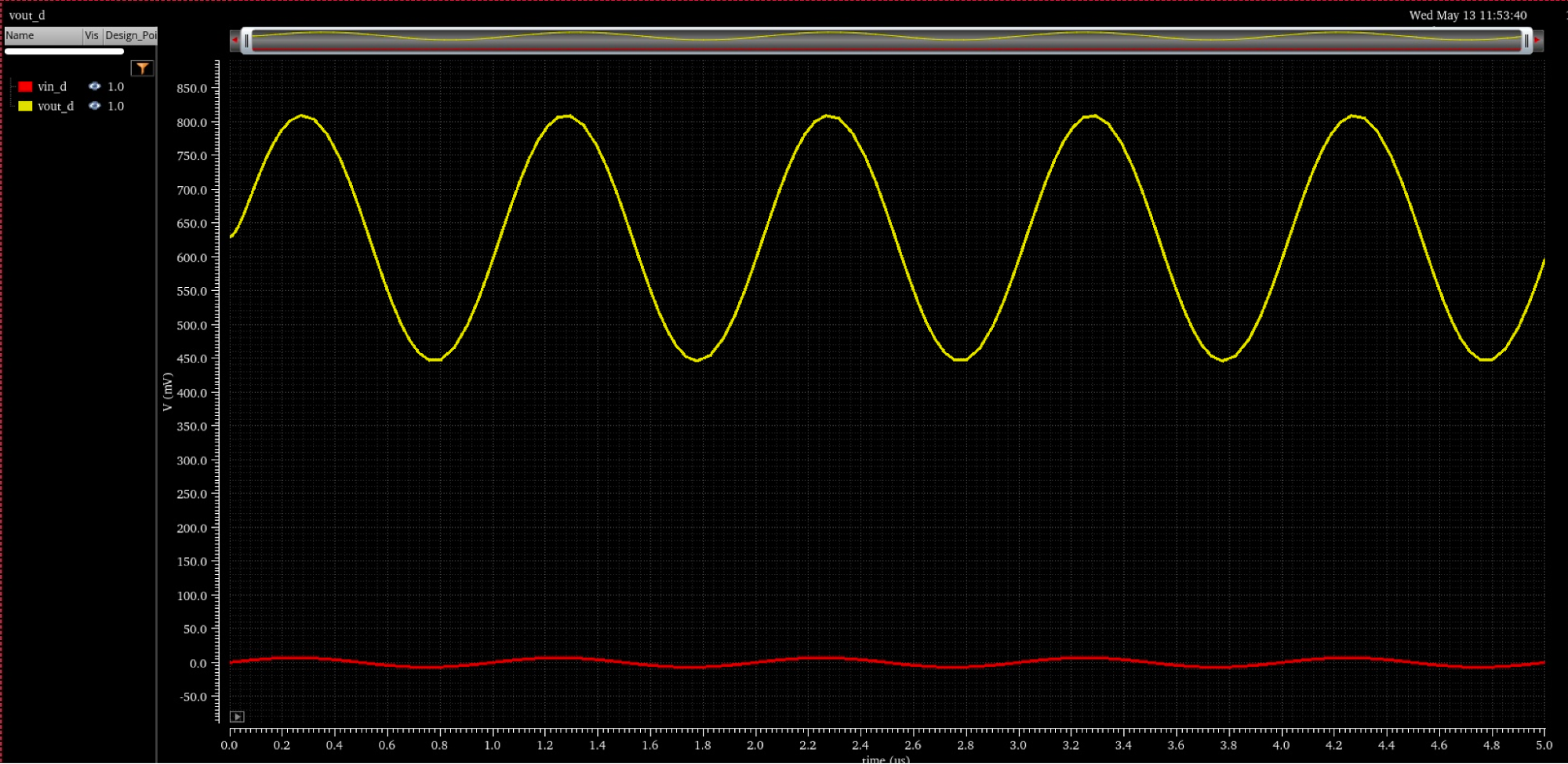
Transient response: VOUT vs VIND at 1 MHz
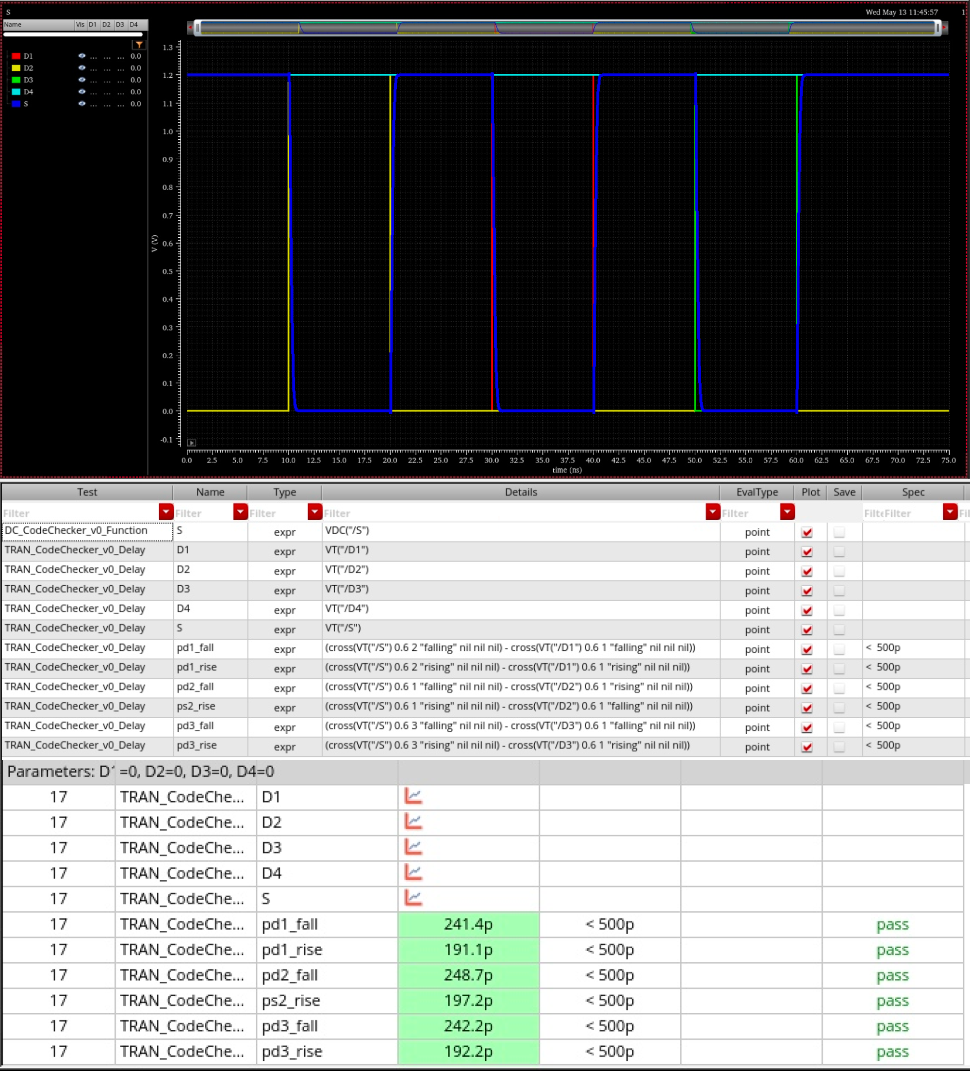
Address decoder timing: input switching vs enable transition