NAND-Gate Logic Demo PCB
KiCad
PCB Design
Board Bring-Up
Power Integrity
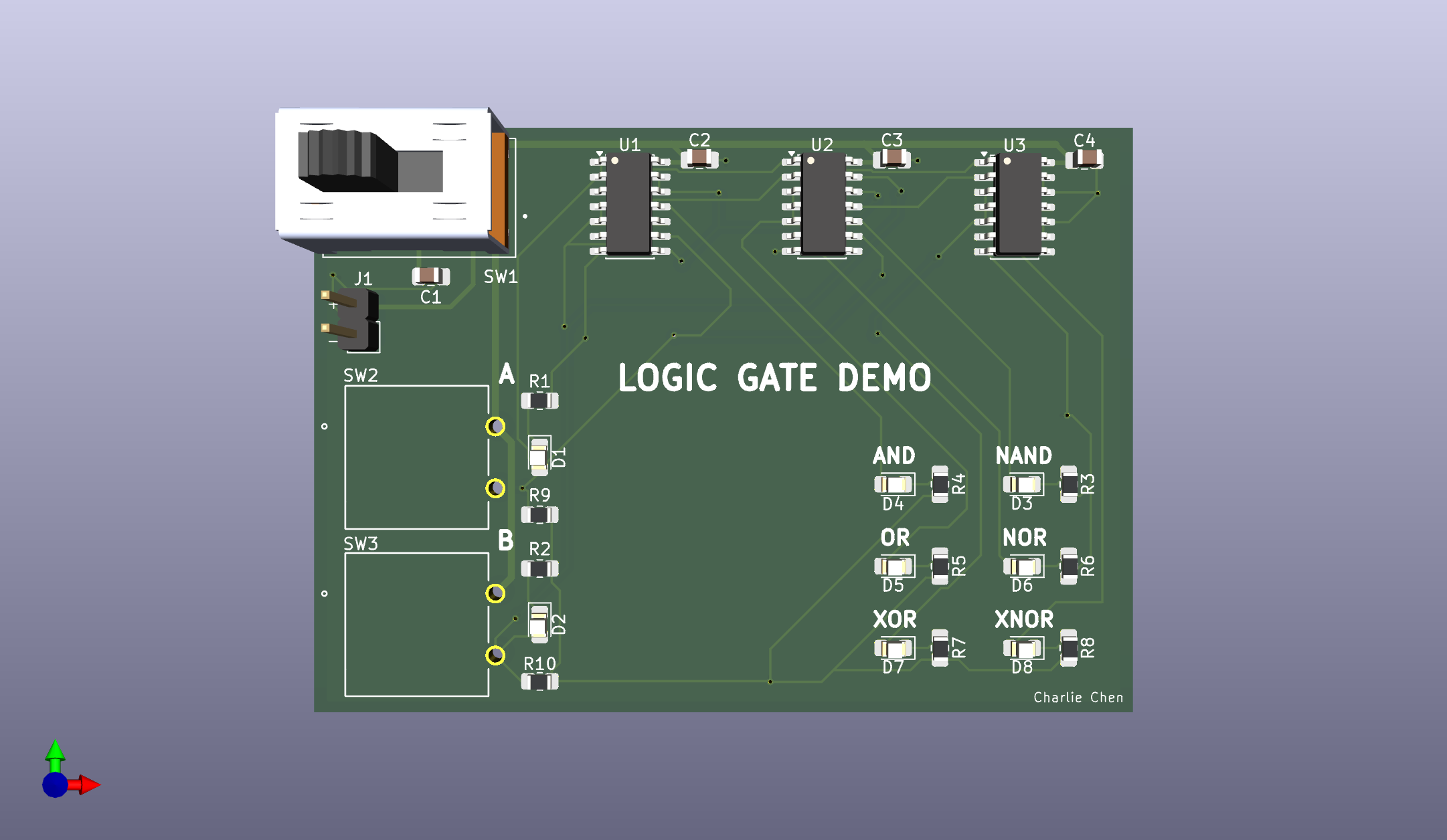
A 2-layer PCB designed to demonstrate functional completeness by implementing all six core Boolean functions (NOT, AND, OR, NOR, XOR, XNOR) using only 74HC00 quad NAND gate ICs. The project served as a practical exercise in discrete logic design, KiCad layout, power integrity, and physical board bring-up.
Circuit & Logic Design:
- Universal Gate Topology: Wired 74HC00 quad 2-input NAND gates into equivalent schematics for NOT, AND, OR, NOR, XOR, and XNOR functions.
- Input/Output Hardware: Integrated tactile switches and DIP switches with explicit pull-up/pull-down resistors to guarantee clean, deterministic logic inputs, with LED indicators displaying output states.
Power & Signal Integrity:
- Decoupling Strategy: Placed 0.1 µF ceramic decoupling capacitors directly adjacent to the VCC pin of each IC to suppress switching noise and prevent local VDD droop during fast input transitions.
- Ground Return Paths: Maintained a continuous, uninterrupted ground plane on the bottom layer to minimize return loop inductance and prevent ground bounce across multiple simultaneously switching gates.
Assembly & Board Bring-Up:
- Hand Assembly & Inspection: Soldered components and inspected power rails for shorts prior to initial power-on.
- Hardware Validation: Verified static logic thresholds (VIL, VIH, VOL, VOH) with a multimeter and tested all 64 input combinations across the logic gates to ensure clean, glitch-free operation.
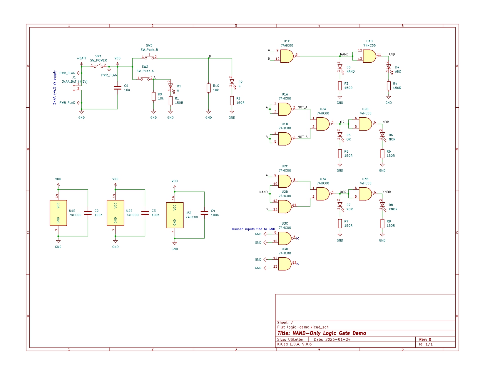
KiCad schematic showing NAND gate configurations for all 6 logic functions.
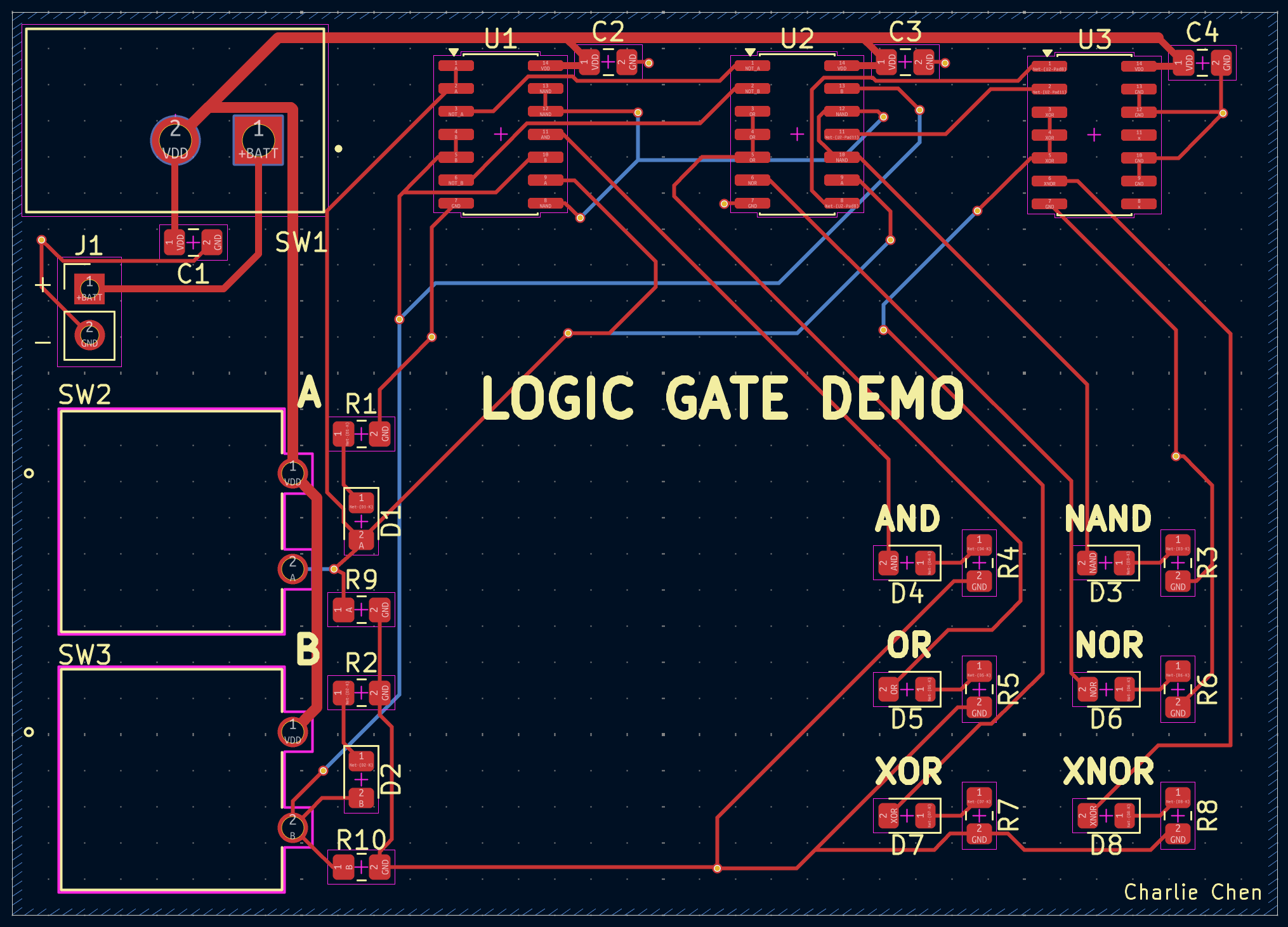
2-layer PCB layout highlighting continuous ground plane and decoupling capacitor placement.

Physical board bring-up and logic level verification.