Multicycle MIPS Processor & Assembler
SystemVerilog
RTL Design
Xilinx Vivado
FPGA
FSM Control
Testbenches
Python
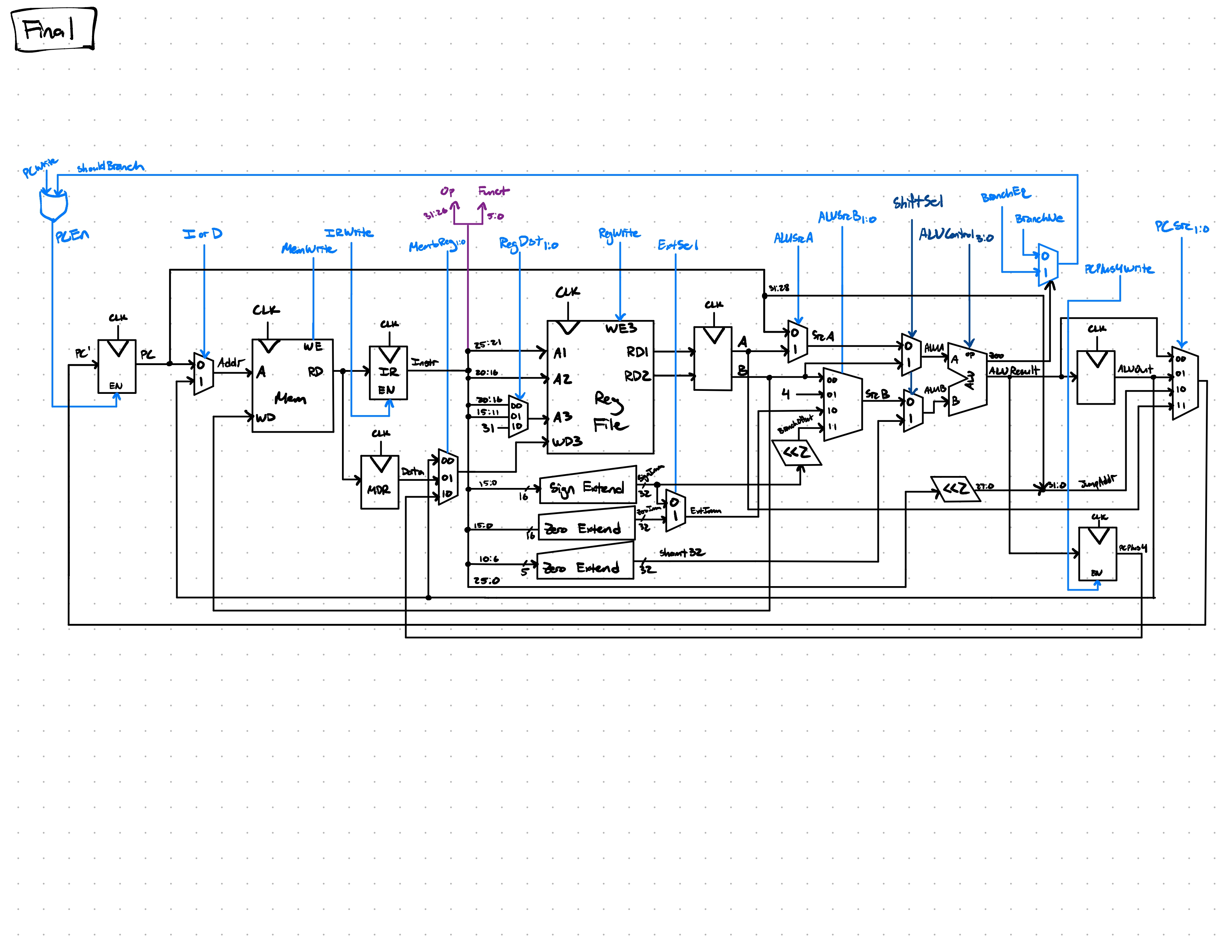
A multicycle MIPS CPU designed in SystemVerilog and deployed to an FPGA. The architecture trades control path complexity for hardware efficiency, reusing core hardware components—such as a single ALU and unified memory interface—across variable clock cycles per instruction.
Datapath & Architecture:
- Resource-Shared Datapath: Routed ALU, register file, and memory buses through intermediate registers (IR, MDR, A, B, ALUOut). Reused the primary ALU for both PC branch target calculation and arithmetic operations across 3-to-5-cycle execution windows.
- Instruction Set Support: Implemented datapath routing and control logic for R-type (e.g., ADD, SUB, SLT), I-type (e.g., LW, SW, BEQ), and J-type (e.g., J) instruction classes.
FSM Control Path:
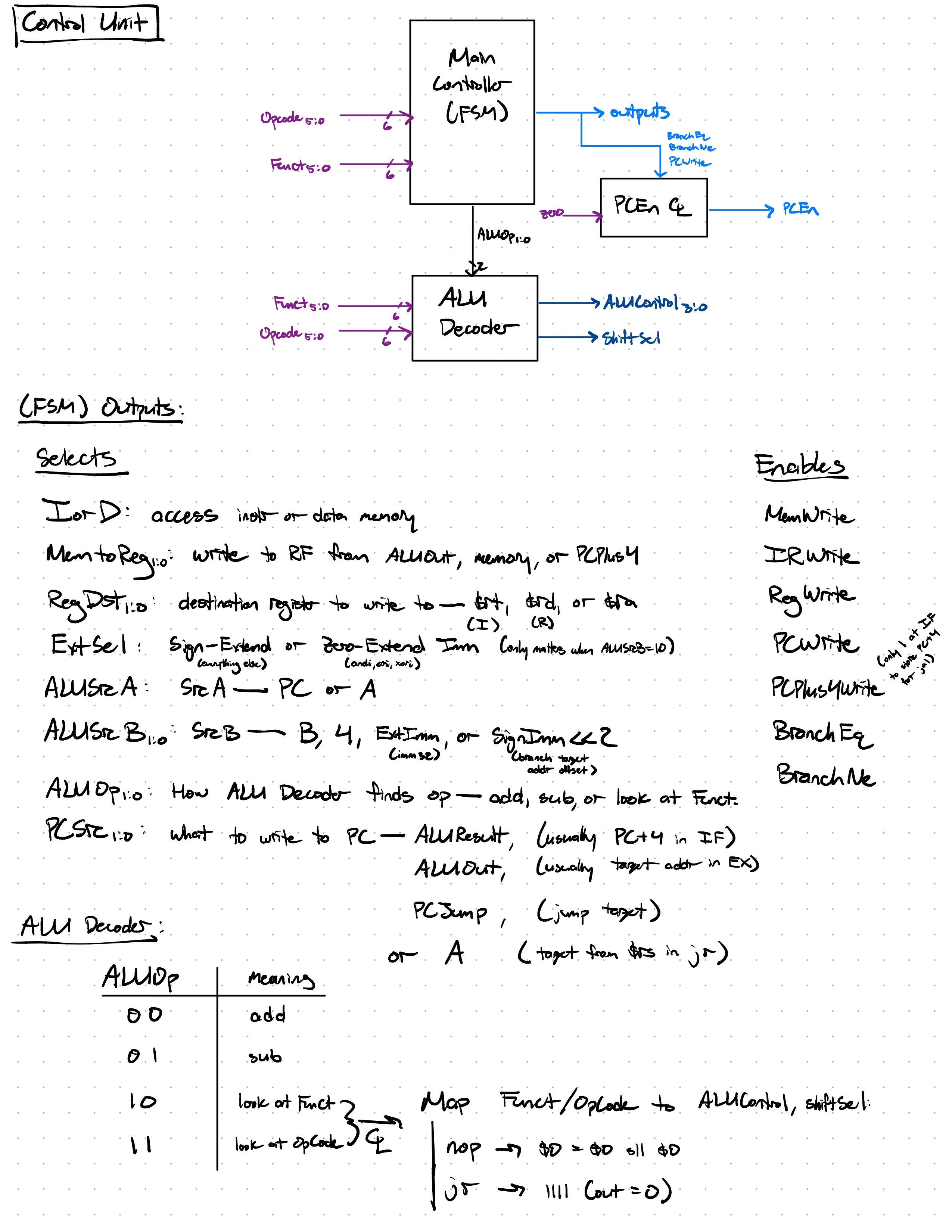
- Multi-State Control Unit: Designed a central finite state machine to sequence control signals across instruction fetch, decode, execution, memory access, and write-back states.
- Branch & Jump Control: Built control path logic to calculate branch offsets and evaluate condition flags during decode steps, ensuring deterministic execution for conditional jumps and branches.
Toolchain & FPGA Hardware Bring-Up:
- Cycle-Accurate Simulation: Verified control outputs, memory writes, and register state transitions in Xilinx Vivado using testbenches and waveform analysis.
- Assembler & FPGA Deployment: Wrote a custom Python assembler to compile assembly files into machine code binaries, using a loader script to write instructions into FPGA memory for real-time execution testing.
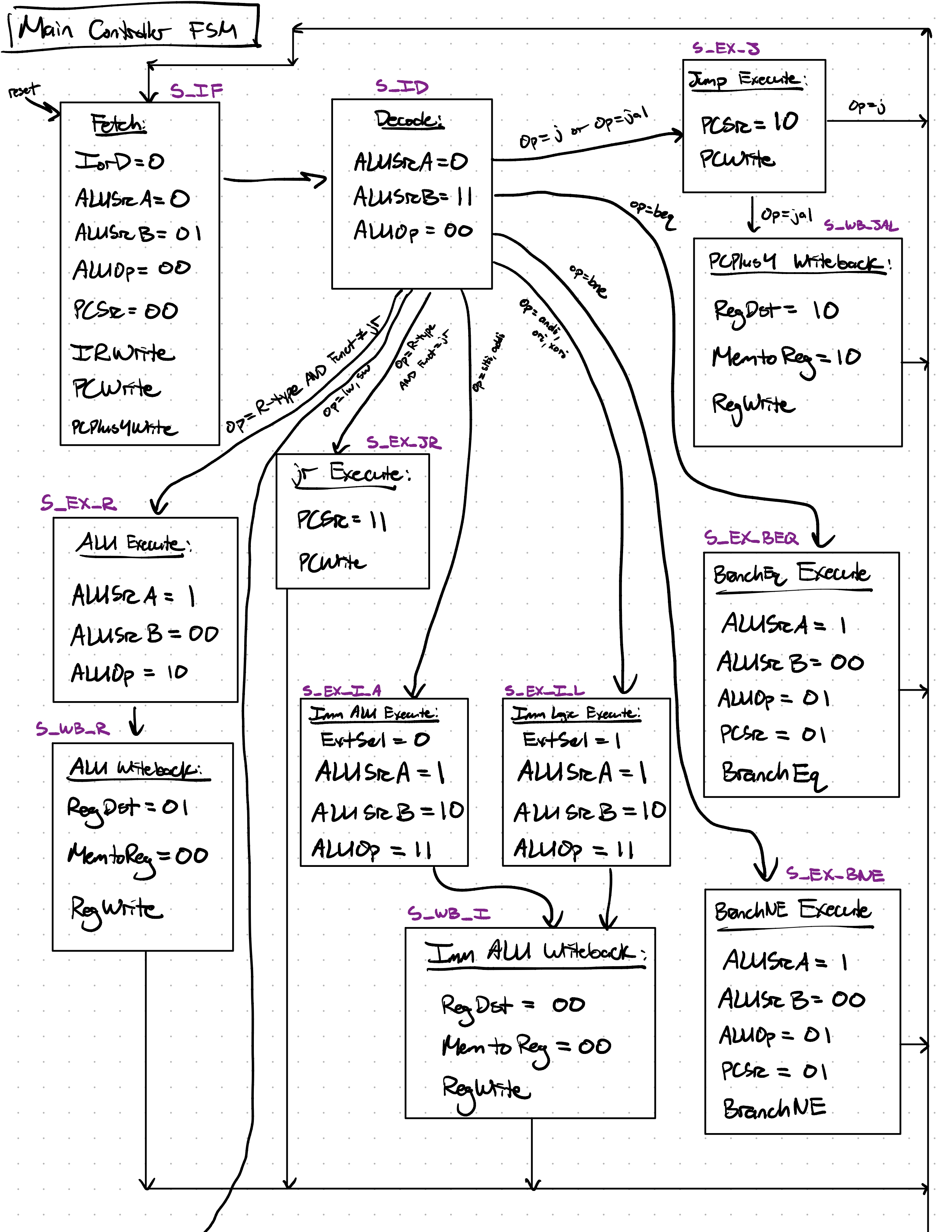
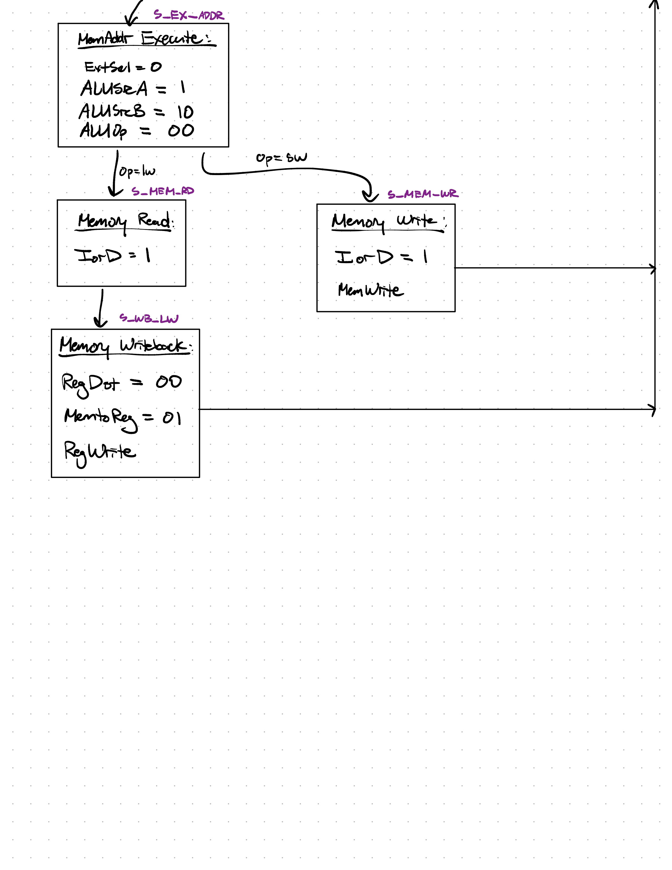
FSM control state diagram for multicycle instruction sequencing.